Heidelberg Instruments Mikrotechnik GmbH
Description
We are a manufacturer of extreme high resolution Laser Lithography Tools. These systems are used for writing structures in a sub micron range with nanometer precision! a world leader in design, development and manufacturing of advanced laser based maskless lithography systems for production of photomask, as well as laser direct imaging.
Applications include: Micro and Nano technology, MEMS, Displays, Advanced Packaging, ASICS, Micro Optics, and many other related fields.
Tell your friends
RECENT FACEBOOK POSTS
facebook.comTimeline Photos
Happy Holidays
SEMICON West 2016
Visit Heidelberg Instruments at Semicon West this week July 12-14 Booth 2623 http://expo.semi.org/west2016/public/eBooth.aspx?IndexInList=215&FromPage=Exhibitors.aspx&ParentBoothID=&ListByBooth=true&BoothID=322544
RIT Engineering Laboratory receives high tech system from Heidelberg Instruments to improve...
http://www.himt.de/index.php/news-reader/items/rit-engineering-laboratory-receives-high-tech-system-from-heidelberg-instruments-to-improve-lithographic-process-for-semiconduct.html
www.azonano.com
CPI and Heidelberg Instruments Develop New Roll to Roll Digital Lithography Tool to Commercialize OTFTs The Centre for Process Innovation (CPI) and Heidelberg Instruments have announced that they have developed a new high resolution, high speed roll to roll digital lithography tool for the manufacture of flexible organic thin film transistors (OTFT) used in next generation applications such as foldable display screens, sensors, integrated circuits and photo-detectors. http://www.azonano.com/images/news/NewsImage_34368.jpg http://www.azonano.com/news.aspx?newsID=34368
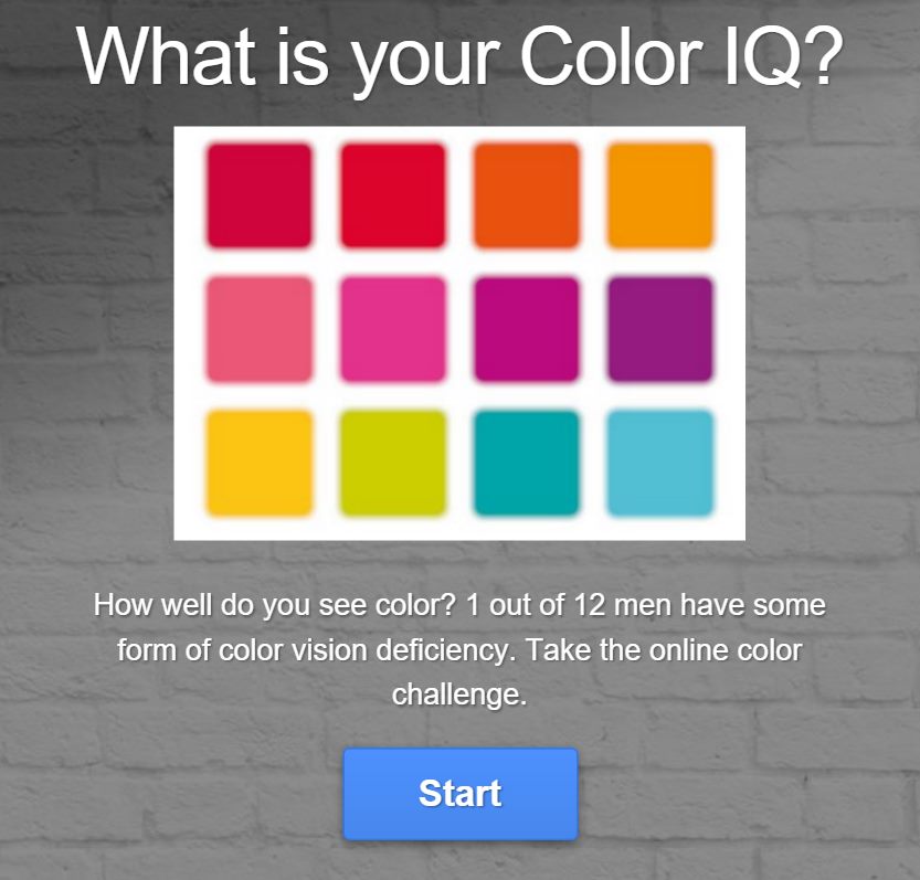
Quiz